Every package warps during reflow.
Which solder
joints are
at risk?
Assembly warpage, joint by joint.
SiFlux reads your layout, replays the assembly step by step in full 3D, and checks every solder pad at its bonding step: which pads are flagged, and how much margin a design change gives them. In minutes, on one GPU workstation.
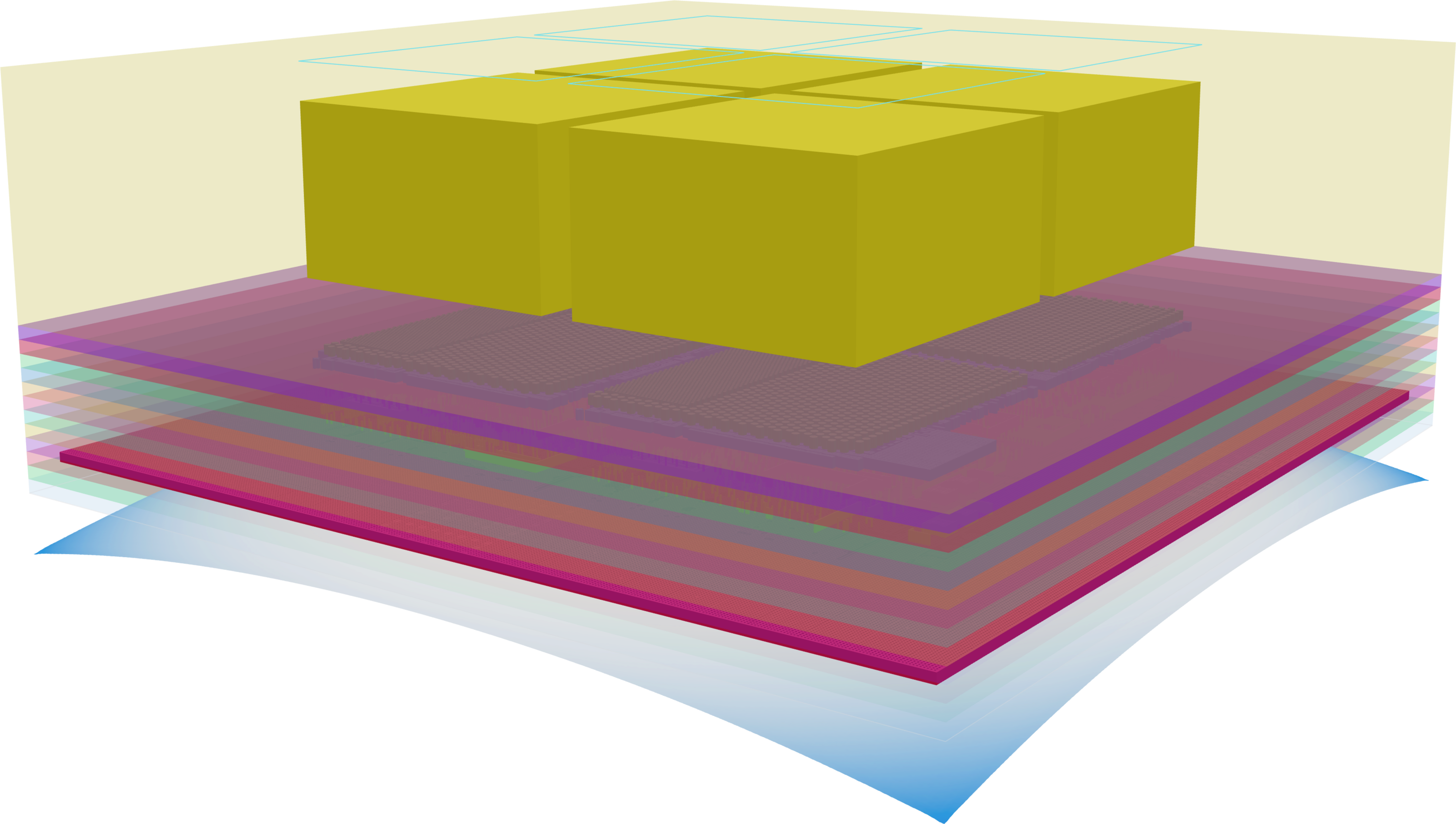
Released from its carrier, the package takes its own shape. Bend drawn 32×.
01 / DECIDE
Can a different film reduce solder joint risk?
Same package. A film that expands less when heated.
- 8 mmflip chip
- 12 mmsubstrate
- 1,600solder bumps
Illustrative example · chip attach, 221 °C · screening result, not a yield prediction
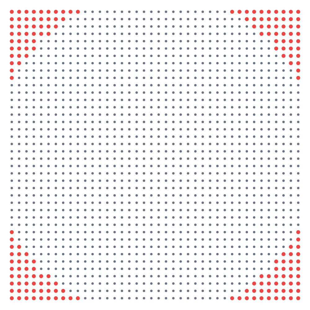
184 pads flagged
of 1,600 solder bumps
198 µm warpage at 25 °C
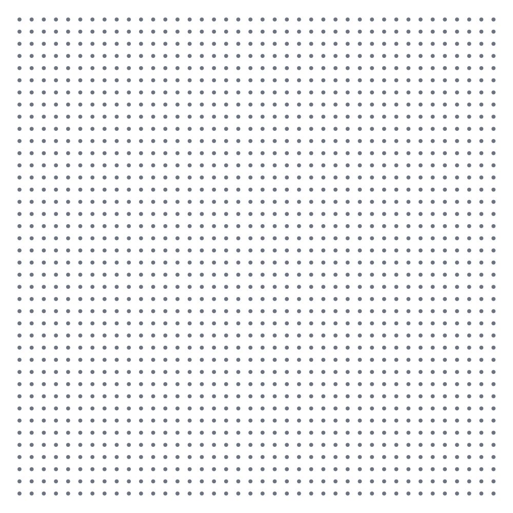
0 pads flagged
11.3 µm opening margin
95 µm warpage at 25 °C
Will the solder form a connection?
If bending leaves too large a gap, the solder cannot connect the two metal pads.
Connection possible
Positive margin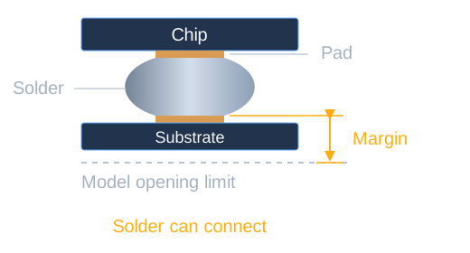
Gap prevents connection
Pad flagged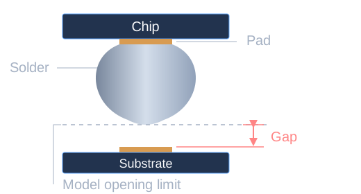
Opening margin: how much more the pads can separate.
Illustrative · not to scale · geometric screening, not yield
Compare solder connection risk
Pads flagged (count)
Film thermal expansion · ppm/K
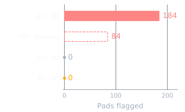
45, 35 & 30 ppm/K: full 3D.
Opening margin (µm)
Film thermal expansion · ppm/K
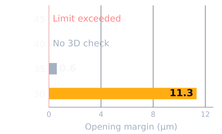
Larger margin = more separation allowed.
FROM LAYOUT TO JOINTS / LAYOUT
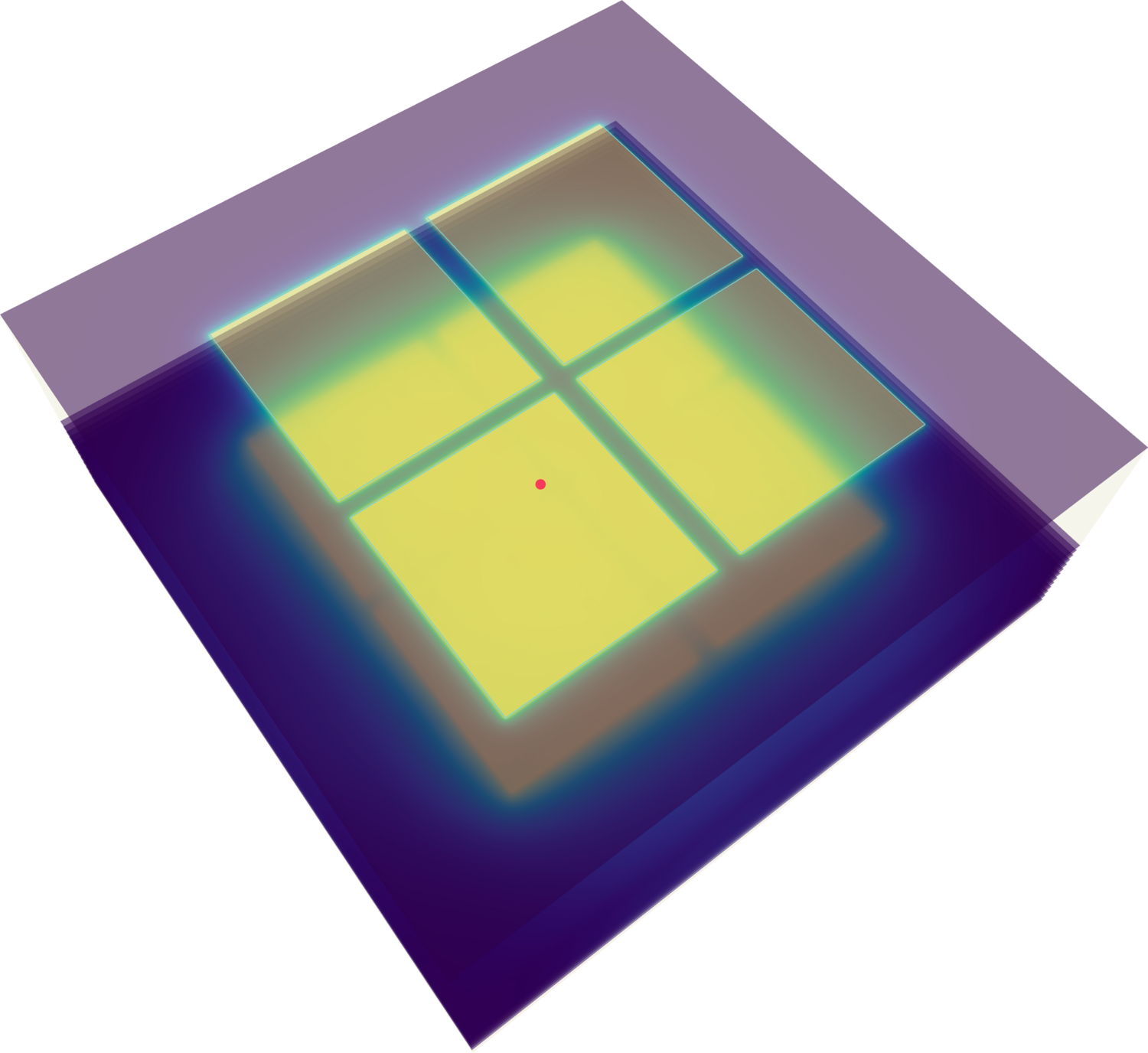
Your layout is the model
Import GDS or OASIS layouts. This demo has nine copper layers, 8,920 micro-bumps and 678 solder balls. The 24-million-node grid, 16 µm, builds itself.
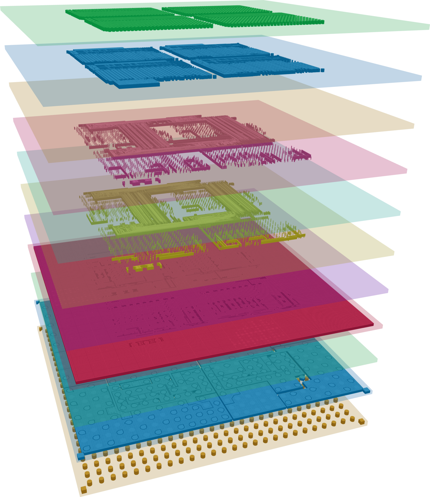
FROM LAYOUT TO JOINTS / THERMAL
Hotspot 98.8 °C
Steady state, 40 W in four dies under a heat sink. 24 million nodes: solver 15.0 s, click to result 19 s.
FROM LAYOUT TO JOINTS / ASSEMBLY
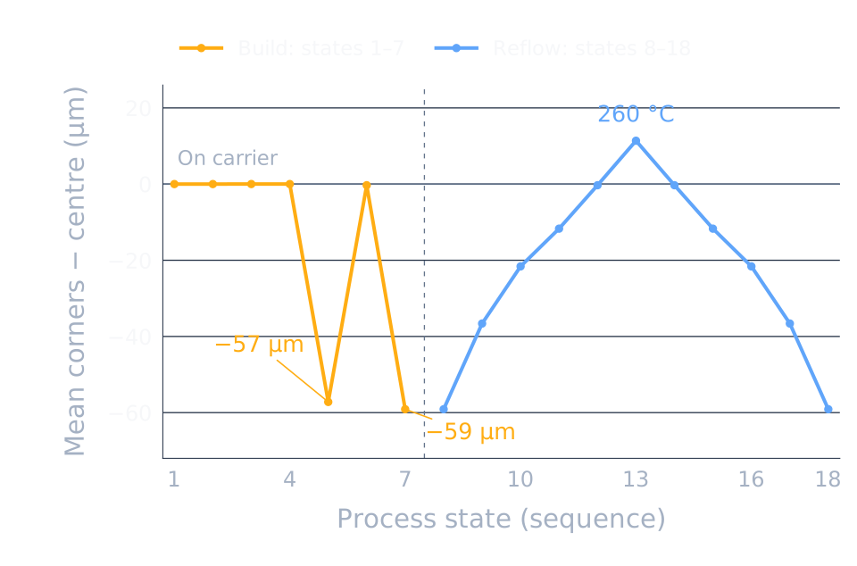
Predict warpage through the full assembly process
From package build through solder reflow and cooling. 18 states in full 3D; click to result 4.0 min.
FROM LAYOUT TO JOINTS / JOINTS
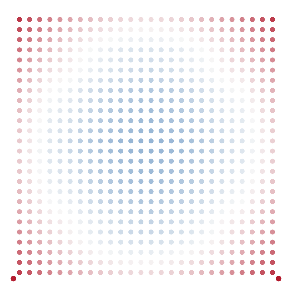
678 pads, none flagged
Solder balls at board reflow, by gap change: blue closes, red opens, ±2.0 µm. Minimum opening margin 35.1 µm.




Examples use representative material values and assumed power and cooling; linear elastic, prescribed process temperatures, rigid carrier and flat board assumed. “Pads flagged” is a screening result, not a yield prediction.